
EN
EN

PbS,PbSe,PbTe
Lead compounds (PbS, PbSe and PbTe) are direct-bandgap semiconductor materials, whose applications are limited to infrared detection and thermal imaging. These semiconductors operate at wavelengths ranging from 1 to 5.5 μm. They perform well at room temperature, but cooling can be applied when higher sensitivity is required. PbTe, PbSe and PbS detectors are widely used in flame detection, combustion control, non-contact temperature measurement, gas and humidity monitoring, spectrophotometry, analytical testing and medical imaging.
Basic Material Properties
Material | PBS | PbSe | PbTe |
Structure | Cubic (NaCL-type) | ||
Density | 7.60g/cm³ | 8.15 g/cm³ | 8.16 g/cm³ |
Thermal conductivity (at 25 °C) | 0.03 W/cmK | 0.017 | 0.017 |
Refractive index (λ = 6 μm) | 4.19 | 4.54 | 5.48 |
Direct bandgap | 0.37 eV | 0.27 eV | 0.32 eV |
Maximum crystal diameter / length | ∅ 38.1×40mm | ∅25.4×40mm | ∅25.4×40mm |
Processing Parameters
Diameter / Width | 55mm |
Thickness / Length | 0.1-30mm |
Surface Quality | 80/50, 60/40, 40/20 |
Direction | (100) |
We can supply PbS, PbSe and PbTe rods, wafers and slices. Please contact us for customization requirements.
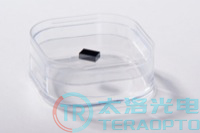
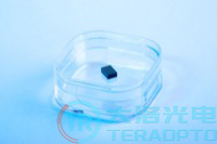
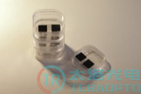
Other specifications can be customized upon request.