
EN
EN
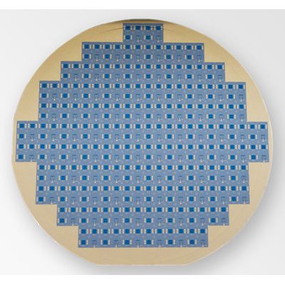
Customized epitaxial growth of LT-GaAs (low-temperature gallium arsenide) substrates
GaAs (gallium arsenide) is a compound of Group III-V elements, appearing as a black-gray solid with a melting point of 1238°C. It remains stable in air below 600°C and is resistant to corrosion by non-oxidizing acids. Gallium arsenide serves as a semiconductor material characterized by high electron mobility, low dielectric constant, ability to incorporate deep-level impurities, small effective electron mass, unique band structure, and suitability for epitaxial growth.
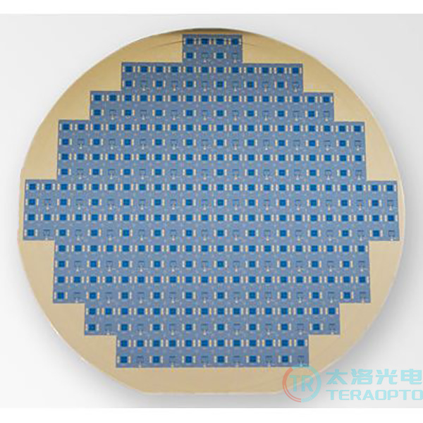
1、Structural Growth of Semiconductor Optoelectronic Devices
We can grow high-quality epitaxial thin film layers of AlAs, GaAs, InAs, AlGaAs, AlInAs, and InGaAs on GaAs substrates, suitable for various applications.
2、Low-temperature gallium arsenide
For applications requiring rapid response devices, such as optical detectors, saturable absorbers, or photoconductive antennas, we offer low-temperature epitaxial growth devices with response times as short as 1 ps.
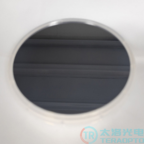
We provide one or two single layers of low-temperature gallium arsenide grown on GaAs substrates.
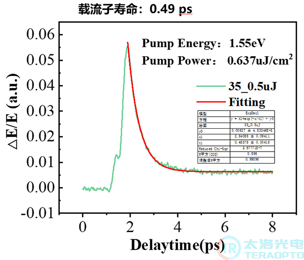
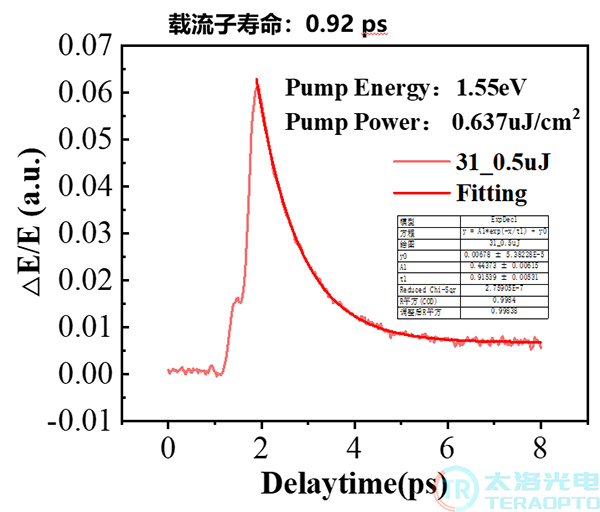
The parameters are as follows:
Gallium arsenide wafer diameter: 2" or 4"
Maximum film stack thickness: 5 μm
specifications:
LT-GaAs-50.8:2"(50.8 mm)LT-GaAs wafer
LT-GaAs-100:4"(100 mm)LT-GaAs wafer
LT-InGaAs-100:4"(100 mm)LT-InGaAs wafer
LT-GaA-100-C:4"(100 mm)LT-GaAs wafer with a custom metal structure
For specific specifications, please inquire further.